Academic Degrees
- Ph.D., Solid-State Physics, Swiss Federal Institute of Technology (ETH), Zürich, Switzerland.
- M.S., Physics, Swiss Federal Institute of Technology (ETH), Zürich, Switzerland.
Certifications
- PhD
Breaking News...
Areas of Research and Professional Interest
- 2D Materials: Metal chalcogenide semiconductors, graphene, hexagonal boron nitride, heterostructures of 2D/layered materials: Fundamental growth mechanisms, scalable synthesis; electronic structure, optoelectronic properties, charge transport; defect chemistry & functionalization; devices for electronics, energy applications, sensing.
- Nanomaterials: Semiconductor nanowires & nanowire heterostructures; nanoscale heterostructures (in-plane structures & vertical stacks) of 2D materials; programmable self-assembled supra-crystalline architectures built from nanoparticle components.
- Energy conversion & energy efficiency: Energy harvesting & photovoltaics.
- Advanced methods development: In-situ and microscopy & spectroscopy; low-energy & photoelectron microscopy; advanced electron microscopy techniques, high-resolution cathodoluminescence spectroscopy in STEM; scanning probe microscopy & spectroscopy; electron and scanning probe microscopy & spectroscopy at elevated gas pressures and in liquids.
In the News: Powered by the 
Inventions/Patents
- “Assembly of Ordered Carbon Shells on Semiconducting Nanomaterials”, U.S. Patent No. 7,714,317 (issued May 11, 2010).
- “Apparatus for Dispensing Material”, U.S. Patent No. 7,972,560 (issued July 5, 2011).
- “Segmented Nanowires Displaying Locally Controllable Properties”, U.S. Patent No. 8,389,387 (issued March 5, 2013).
- “Assembly of Ordered Carbon Shells on Semiconducting Nanomaterials”, U.S. Patent No. 8,278,124 B2 (issued October 2, 2012).
- “Processing of Monolayer Materials via Interfacial Reactions”, U.S. Patent No. 8728433 (issued May 20, 2014).
- “Stable and Metastable Nanowires Displaying Locally Controllable Properties”, U.S. Patent No. 8890115 (issued November 18, 2014).
- “Monolayer and/or Few Layer Graphene on Metal or Metal-Coated Substrates”, U.S. Patent No. 9006644 (issued April 14, 2015).
- “Method for Forming Monolayer Graphene-Boron Nitride Heterostructures”, U.S. Patent No. 9,410,243 (issued August 9, 2016).
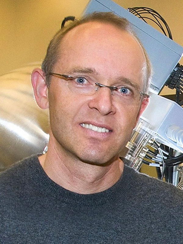
About Peter Sutter
Peter Sutter joined UNL in 2015 after 11 years at the Center for Functional Nanomaterials at the Brookhaven National Laboratory, where he was a staff scientist, research group leader and facility leader. His research interests include 2D materials, interfacial physics and chemistry, nanomaterials and advanced instrument and methods development. He was an associate and assistant professor in physics at the Colorado School of Mines and earned doctoral and bachelor’s degrees from the Swiss Federal Institute of Technology (ETH Zürich).
Honors and Awards
2015 Battelle Inventor of the Year
2015 Long Island Technology Hall of Fame - Patent of the Year
2014 General Chair, International Conference on Nanoscience + Technology 2014
2013 Executive Committee Member, Surface Science Division of the American Vacuum Society
2011 Science Editor’s Choice: “Reflecting Atoms off Graphene”
2011 Sapphire Prize, Journal of Materials Research/Springer
2010 Thomson Reuters - Highly Cited Paper on Epitaxial Graphene
2007 Scientific American 50 Award for Leading Contributions to Science and Technology
2004 American Physical Society Top Physics Discoveries of the Year
2000 US National Science Foundation CAREER Award
1999 Research Corporation Research Innovation Award
1997 Swiss National Science Foundation Postdoctoral Fellowship
1995 European Materials Society Young Scientist Award
Selected Publications
- A. Castellanos-Gomez, X. Duan, Z. Fei, H. Rodriguez Gutierrez, Y. Huang, X. Huang, J. Quereda, Q. Qian, E. Sutter, and P. Sutter, “Van der Waals Heterostructures”, Nature Reviews Methods Primers 2, 58 (2022).
- Y. Huang, Y. Pan, R. Yang, L. Bao, L. Meng, H. Luo, Y. Cai, G. Liu, W. Zhao, Z. Zhou, L. Wu, Z. Zhu, M. Huang, L. Liu, L. Liu, P. Cheng, K. Wu, S. Tian, C. Gu, Y. Shi, Y. Guo, Z. Cheng, J. Hu, E. Sutter, P. Sutter, Y. Wang, W. Ji, X. Zhou, and H.-J. Gao, “Universal Mechanical Exfoliation of Large-Area 2D Crystals”, Nature Communications 11, 2453 (2020).
- P. Sutter, S. Wimer, and E. Sutter, “Chiral Twisted van der Waals Nanowires”, Nature 570, 354-357 (2019).
- P. Sutter, R. Ibragimova, H.-P. Komsa, B.A. Parkinson, and E. Sutter, “Self-Organized Twist-Heterostructures via Aligned van der Waals Epitaxy and Solid-State Transformations”, Nature Communications 10, 5528 (2019).
- E. Sutter, P. Sutter, A.V. Tkachenko, R. Krahne, J. de Graaf, M. Arciniegas, and L. Manna, “In Situ Microscopy of the Self-Assembly of Branched Nanocrystals in Solution”, Nature Communications 7, 11213 (2016).
- A. Rahman, A. Ashraf, H. Xin, X. Tong, P. Sutter, M.D. Eisaman, and C.T. Black, “Sub-50 Nanometer Self-Assembled Nanotextures for Enhanced Broadband Antireflection in Silicon Solar Cells”, Nature Communications 6, 5963 (2015).
- E. Sutter, K. Jungjohann, S. Bliznakov, A. Courty, E. Maisonhaute, and P. Sutter, “In-situ Liquid Cell Electron Microscopy of Ag-Pd Galvanic Replacement Reactions on Ag Nanoparticles”, Nature Communications 5, 4946 (2014).
- G. Nazin, Y. Zhang, L. Zhang, E. Sutter, and P. Sutter, “Visualization of Charge Transport through Landau Levels in Graphene”, Nature Physics 6, 870 (2010).
- P. Sutter, “Epitaxial graphene: How silicon leaves the scene”, Nature Materials 8, 171 (2009).
- P. Sutter, J.I. Flege, and E. Sutter, “Epitaxial Graphene on Ruthenium”, Nature Materials 7, 406 (2008). [Thomson-Reuters highly cited paper]
- P. Sutter and E. Sutter, “Dispensing and Surface-Induced Crystallization of Zeptoliter Liquid Metal Alloy Drops”, Nature Materials 6, 363 (2007). [Scientific American 50 Award. Featured in print: San Francisco Chronicle, Physics Today, Science News, Chemical & Engineering News, Chemistry World (Royal Society for Chemistry), Materials Today, R&D Magazine. On the web: Science Shots (Science, AAAS), MRS Material News, www.weltderphysik.de (German Physical Society), www.azonano.com, www.physorg.com, www.chemie.de, and many more]