Congratulations to Ying on her successful comprehensive exam
April 2019
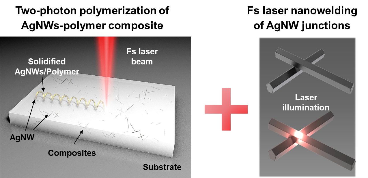
Precise Assembly and Welding of Silver Nanowires in Three Dimensions for Multifunctional Device Fabrication
Three dimensional (3D) electrically conductive micro-/nano structures is are now a key component in a broad range of research and industry fields. Nevertheless, current methods of fabricating metallic microstructures, including inkjet, selective plating, metallic inversion, and in-situ photoreduction, have a realistic limit of the simultaneous realization of conductive 3D microstructures with controllable morphology and desired conductivity. Meanwhile, a bottleneck in reducing the junction-to-junction resistance exists to achieve desired conductivity and functionality. Aiming to create multi-functional structures and devices for various of applications, the overall objective of the proposed research is to develop a new additive manufacturing process based on flexible femtosecond laser direct laser writing (FsDLW) via two-photon polymerization (TPP) and laser nanowelding. The project objectives are: 1) Design, preparation and fabrication of novel conductive silver nanowire (AgNW)-polymer composites; 2) Femtosecond laser-induced nanowelding of AgNW junctions inside the composites to reduce the junction resistance; 3) Investigation of conductive mechanism of the composites; and 4) Demonstration of high-performance applications, including 3D electronics, temperature sensors, plasmonic devices.
Scientifically, the success of the proposed research will bring substantial impact to the fundamental understanding of multifunctional nanocomposite materials, providing a method to achieve the user-defined arbitrary 3D structuring with superior electrical conductivity, opening a new arena in disciplines of material science, nanotechnology, and electronics. Technologically, due to the unique and reliable assembly method of AgNWs, our proposed AgNW-polymer composites will potentially overcome the fabrication complexity, the resolution-conductivity tradeoff, and device-to-device variation issues which are the main challenges in current 3D metallic micro/nano fabrication techniques.